logo
productos
Hogar / Productos / Bandejas de JEDEC IC /

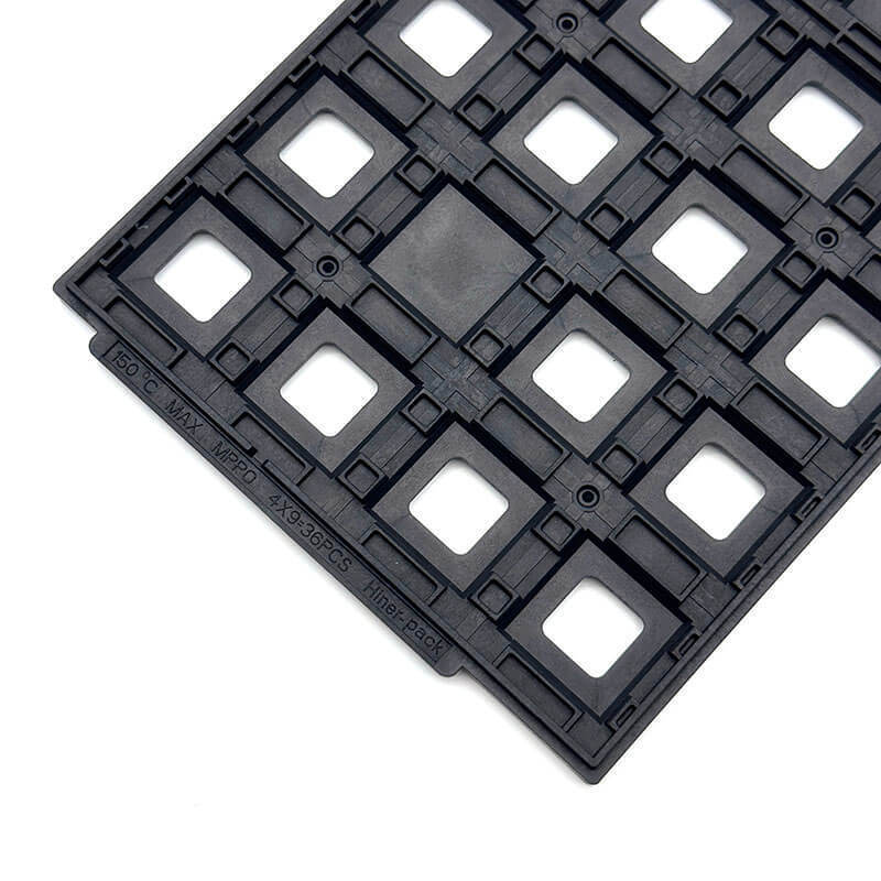
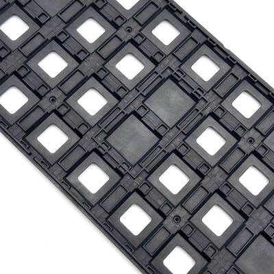
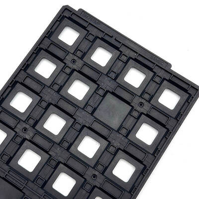
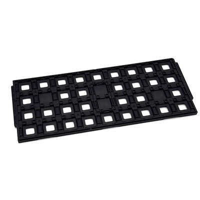
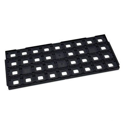
Durable JEDEC IC Trays for Dust-Free Semiconductor Packaging

Durable JEDEC IC Trays for Dust-Free Semiconductor Packaging

Nombre De La Marca: Hiner-pack
Número De Modelo: HN25006
Cuota De Producción: 500 piezas
Precio: $1.35~$2.38(Prices Are Determined According To Different Incoterms And Quantities)
Condiciones De Pago: T/T
Capacidad De Suministro: 2000 unidades/día
Información detallada
Lugar de origen:
Porcelana
Certificación:
ROHS, ISO
Tray Weight:
Varía, normalmente hasta 500 gramos por cavidad
Color:
Negro
Seguro de calidad:
Garantía de entrega, calidad fiable
Tamaño de la cavidad:
322,6x135,9x7,62mm
Incoterms:
EXW, FOB, CIF, DDU, DDP
Tipo de molde:
Inyección
Reutilizable:
Forma de la bandeja:
Rectangular
Clase limpia:
Limpieza general y ultrasónica
Tipo de circuito integrado:
BGA,QFP,QFN,LGA,PGA
Nivel de embalaje:
Paquete de transporte
Llanura:
Menos de 0,76 mm
Capacidad:
4x9=36 UDS.
Detalles de empaquetado:
cartón, paleta
Capacidad de la fuente:
2000 unidades/día
Descripción del producto
Durable JEDEC IC Trays for Dust-Free Semiconductor Packaging
Shield delicate semiconductor components from dust and damage during packaging operations. Minimize contamination risks effectively. Built with durable structure to meet JEDEC standards for reliable industrial use. Seeking trusted tray solutions for secure semiconductor packaging?

Fit automated packaging lines and cleanroom environments perfectly. Perform steadily in component handling and packaging procedures. Adapt to diverse semiconductor packaging processes smoothly.

Enable safe component storage and logistics. Support custom designs to meet specific packaging demands. Deliver tailored solutions for unique semiconductor manufacturing requirements.
Key Features/ Benefits 
  • Deliver durable construction.
  • Reduce dust contamination.
  • Dust minimization.
  • Component protection.
  • Flexible customization.
Specifications
Brand Hiner-pack
Model HN25006
Material  MPPO
Package Type JEDEC
Color Black
Resistance 1.0×10⁴ - 1.0×10¹¹ Ω
Outline Line Size 322.6x135.9x7.62 mm
Cavity Size 16×9.5×4.72 mm
Matrix QTY 4x9=36 PCS
Warpage MAX 0.76mm
Service Accept OEM, ODM
Custom Pocket Options Available
Applications
Apply to semiconductor wafer level packaging, IC performance testing, die sorting, wafer fabrication, and device assembly. Adapt to cleanroom manufacturing, automated production lines, precision component handling, and high-temperature processing workflows. Ensure stable performance in strict dust-free environments.

Support component long-term storage, inter-factory logistics, production turnover, vacuum packaging, and sample shipment operations. Meet diverse requirements for semiconductor packaging, quality inspection, supply chain management, and electronic component distribution.
Packaging & Shipping/ Services
Offer targeted customization for JEDEC IC trays tailored to packaging and transportation needs. Collaborate closely with teams to design cavity shapes, anti-slip structures, and shock-absorbent materials for secure component handling during packaging and long-distance logistics. Develop anti-static or dust-sealed variants, and validate prototypes through vibration and drop tests. Deliver personalized tray solutions that safeguard semiconductor components throughout packaging, loading, and inter-factory or global shipment processes.
About Us:
Hiner-pack® was founded in 2013. It is a high-tech enterprise that integrates Design, R&D, Manufacturing, Sales of IC packaging and testing, as well as semiconductive wafer fabrication process in automated handling, carrying, and transportation to provide customers with turnkey services.

Why Choose Us:

  • Rich experience in JEDEC / IC / waffle pack trays
  • In-house mold design capability
  • Fast prototype development
  • Strict QC process
  • Stable supply for global semiconductor customers